RCCN WeChat QrCode
 Mobile WebSite
Gate (gate electrode) gate, the meaning of gate, Chinese translation to make a fence, fence. electrode, electrode.
Source (source) source resource, power source, Chinese translation for source. An electrode that functions as a collector.
Drain (drain) drain, leak, Chinese translation is drain. Electrode that plays the role of emission.
Grid
A mesh or spiral electrode composed of metal filaments. One or more electrodes with a fine wire mesh or spiral shape arranged between the anode and the cathode in a multi-electrode electron tube play the role of controlling the intensity of the electric field on the surface of the cathode to change the cathode emission or capture the secondary emission electrons.
Source
The source is referred to as a field effect tube. General transistors are conducted by carriers of two polarities, that is, majority carriers and minority carriers of opposite polarity, so they are called bipolar transistors, while FETs are only conducted by majority carriers. , It is opposite to bipolar type, also called unipolar transistor.
Drain
The drain is in the middle of two highly doped P regions, sandwiching a layer of low doped N region (the N region is generally made very thin), forming two PN junctions. An ohmic contact electrode is made at both ends of the N area, and an ohmic electrode is also made on the two P areas, and the two P areas are connected to form a field effect tube.
How to distinguish between gate source and drain
General transistors are conducted by carriers of two polarities, that is, majority carriers and minority carriers of opposite polarity, so they are called bipolar transistors, while FETs are only conducted by majority carriers. , It is opposite to bipolar type, also called unipolar transistor. It is a voltage-controlled semiconductor device with the advantages of high input resistance (10^8~10^9Ω), low noise, low power consumption, large dynamic range, easy integration, no secondary breakdown phenomenon, and wide safe working area. Has become a strong competitor of bipolar transistors and power transistors
Between the two highly doped P regions, a layer of low doped N regions is sandwiched (the N region is generally made very thin), forming two PN junctions. An ohmic contact electrode is made on both ends of the N area, and an ohmic electrode is also made on the two P areas, and the two P areas are connected to form a field effect tube.
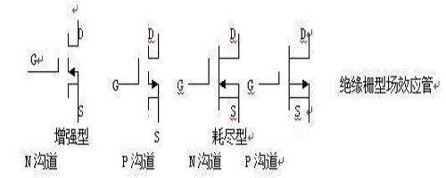
The circuit symbol of N-type conductive channel junction field effect transistor.
Connect the lead wires of the two P areas together as an electrode, called the gate, and lead out an electrode at each end of the N-type silicon wafer, called the source and the drain respectively, and the thin N area is called the conductive groove Tao. Common drain amplifier circuit-source follower
The gate is abbreviated as G, the source is abbreviated as S, and the drain is abbreviated as D.
How to distinguish the source and drain of a 3DJ6 field effect tube
3DJ6 is a domestic N-channel junction field effect transistor, which is usually packaged in a metal round shell (the shape is the same as that of a 3DG6 transistor), and a few are packaged in TO-92. Its appearance and pin arrangement are shown in the figure below.
The shape of the 3DJ6 field effect tube.
The pin arrangement of 3DJ6 field effect tube.
The pin arrangement of 3DJ6 is shown in the figure above. The metal round package is the most common package. The main parameters of the 3DJ6 field effect tube are: the withstand voltage is 20V, the power PD is 100mW, and the size of the drain current IDSS is related to the suffix letter. The suffix letter of the tube is different, and the IDSS is also different. The IDSS of 3DJ6D is 0.35~0.5mA, 3DJ6E is 0.3~1.2mA, 3DJ6F is 1.0~3.5mA, 3DJ6G’s IDSS is 3.0~6.5mA, and 3DJ6H is 6.0~10mA.
Basic application of N-channel junction field effect transistor 3DJ6
Adjustable constant current source circuit composed of 3DJ6.
The 3DJ6 junction field effect tube has high input impedance and low input noise. It used to be used as a low-noise amplifier and impedance converter in the pre-circuit of an amplifier. In the stabilized power supply circuit, the tube is often used instead of constant current diode as a constant current component to improve the stabilized voltage performance of the regulated power supply.
In the above figure, 3DJ6 and resistor R form an adjustable constant current source, and RL is a load resistor (it can be a load such as a Zener tube or LED). This circuit can change the constant current (that is, the current flowing into the load) by adjusting the resistance of R, and the constant current is almost independent of the power supply voltage. When the resistance value of the resistor R is 0Ω, the output constant current is the largest, and this current is the IDSS of the 3DJ6.
If you need a larger constant current, you can use the 3DJ6H with a large IDSS. In addition, if multiple 3DJ6Hs are connected in parallel or bipolar transistors are used to expand the current, a constant current of tens of mA or hundreds of mA can be obtained. The above analysis of the hormone gate, source and drain, I hope to help you in the learning process.